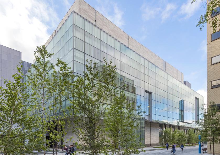
MIT.nano receives LEED Platinum certification

MIT.nano, the Institute’s central, shared-access research facility for nanoscience and nanotechnology, has received the U.S. Green Building Council’s LEED Platinum certification for sustainable practices in new construction.
The Leadership in Energy and Environmental Design (LEED) designation is a performance-based rating system of a building’s environmental attributes associated with its design, construction, operations, and management.
For a leading-edge research center like MIT.nano — which consumes significantly more energy per square foot than a typical office building or traditional laboratory — earning the council’s highest designation of platinum is a remarkable achievement. “MIT.nano’s LEED Platinum certification demonstrates that even the most technically sophisticated buildings can mitigate their environmental impact if sustainability is a priority in the design and construction process,” says Vladimir Bulović, the founding faculty director of MIT.nano and the Fariborz Maseeh Chair in Emerging Technology. “A shared commitment to sustainable principles from the outset made this recognition possible.”
Starting in 2016, MIT made a commitment that all new campus construction and major renovation projects must earn at least LEED Gold certification. MIT.nano joins the Morris and Sophie Chang Building (Building E52) as the second LEED Platinum-certified building on campus. There are 18 total LEED-certified spaces and buildings at MIT.
Recognition is nothing new for the facility, as MIT.nano also received the International Institute for Sustainable Laboratories (I2SL) 2019 “Go Beyond” Award for excellence in sustainability in laboratory and other high-technology facility projects, as well as the R&D World 2019 Lab of the Year Award for excellence in research lab design, planning, and construction, and the AIA New England Honor Award for Design Excellence.
Opportunity beyond the nanoscale
Referred to as the “ship in the bottle” during construction, MIT.nano faced unique challenges due to its location. The building had to rise in the center of a dense urban campus, surrounded on all sides by existing buildings, with very limited access for construction activity and materials. Though constructing the facility was a challenge, the location provides considerable opportunities to connect nanotechnology research to other disciplines and spur new ideas through proximity.
This same mix of challenge and opportunity fueled MIT’s pursuit of its LEED Platinum designation for MIT.nano. Facilities like MIT.nano are resource-intensive: Specialized environments like clean rooms require continuous air exchange, powerful air filtration, precise control and monitoring of temperature and humidity, and other high-energy infrastructure systems to support the diversity of pioneering tools and equipment used.
But the heavy energy requirements of such systems provided a unique opportunity for gains in efficiency. “The energy consumption per square foot of a semiconductor clean room is about an order of magnitude higher than a typical office building. As a result, there is incredible opportunity for innovation during the design process and optimization post occupancy,” says MIT.nano Assistant Director of Infrastructure Nicholas Menounos.
Menounos credits an effort by MIT — including the Department of Facilities and Campus Construction — and the design engineers that went well beyond the typical LEED process. “There was no precedent for a research and development facility of this size, so the team toured around the country, benchmarking against more than 12 peer institutions, to ensure we right-sized the process utilities and HVAC systems,” he says. “Oversizing leads to inefficiencies and undersizing reduces the useful life of the space. This was not a trivial task, and a major reason for the awards.”
Going for platinum
At all levels (certified, silver, gold, and platinum), the LEED certification process is based on a number of points that correlate to sustainability measures. MIT.nano earned points across all seven sections on the LEED scorecard: location and transportation, sustainable sites, water efficiency, energy and atmosphere, materials and resources, indoor environmental quality, innovation, and regional priority. The building notched 84 points total, with 80 points or more needed to earn platinum certification.
MIT.nano rated highly in several categories, including optimizing energy performance, water use reduction, indoor environmental quality, and innovation in design. The building’s overall efficiency is supported by extensive indoor environmental controls and monitoring systems. The clean room, for instance, senses user occupancy with motion and particle detectors and adjusts air recirculation rates accordingly.
“MIT.nano is the most technically complex building on campus with thousands of monitoring points spread throughout the facility,” explains Dennis Grimard, managing director at MIT.nano, in a recent MIT News article. “These points help maintain MIT.nano’s sustainability goals by constantly monitoring the building’s health and operation.”
Those controls account for energy efficiency and stability of research as well as the comfort of occupants. With LEED certification also focused on the health, safety, and well-being of people, additional points were earned through the building’s maximization of open space, use of low-emitting materials, and design efforts to increase natural light throughout the building. “One thing you notice as an occupant is this deep natural light, which isn’t common in labs. While this saves building wattage, it also improves comfort and makes the building a pleasure to be in,” says Menounos.
MIT.nano’s LEED strategy was amplified by MIT’s Central Utilities Plant (CUP), which has a symbiotic relationship with the new facility. The CUP has the opportunity to reuse MIT.nano’s reverse osmosis water in its cooling systems, while MIT.nano relies on the CUP’s distributed energy resource for both thermal and electric energy.
Although the LEED Platinum certification may mark the culmination of a scoring procedure for MIT.nano’s design and construction, Menounos says it does not mark the end of sustainability work and optimization within the building. “Sustainability isn’t a moment in time, it’s a process. Now that MIT.nano is operational, we will continually try to find ways we can change and optimize how the building operates,” he says.

